The PIC 16F877A , AVR ATMEGA 16,32 , ATMEL 89S51 , 52 , ICs used in Arduino uno,mega all are 8 bit microcontrollers.
LPC2148 is more powerful 32 bit uC. It is ARM 7 controller
- On-chip flash programmable memory is 512kb
- It is a high speed controller 60 MHz operation
- Two 10 bit ADC converters provide a total of 14 analog inputs
- One 10- bit D/A converter
- Two 32 bit timers/counters
- 4- CCM (Capture Compare Modulation), 6-PWM, Watchdog timer
- One RTC, 9 interrupts
- One I2C protocol, SPI protocols, SSP protocol
- Two UART serial communication protocols
For development we use KEIL environment.
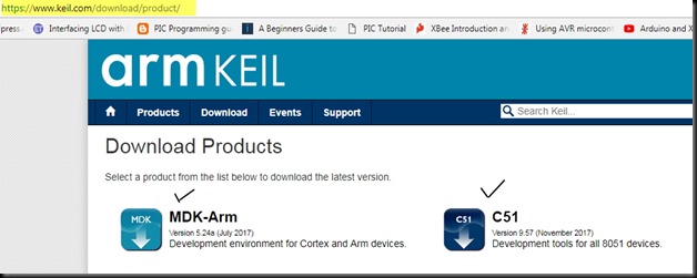
We will use evaluation version of MDK-ARM for C programming. This software is available at
https://www.keil.com/download/product/
Install C51 KEIL & then the MDK-ARM
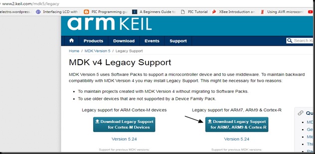
For LPC2148 support you must install the MDK Legacy support files available at
http://www2.keil.com/mdk5/legacy
http://az717401.vo.msecnd.net/legacy/MDK79524.EXE
If this support is not installed , LPC2148 will not show up on the KEIL IC list
Once the installation of KEIL is completed , open up KEIL
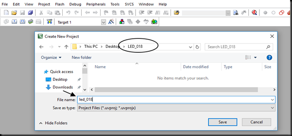
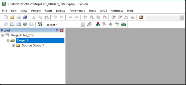
Project –> New uVision Project
Create a Folder for your project & provide a Filename & save.
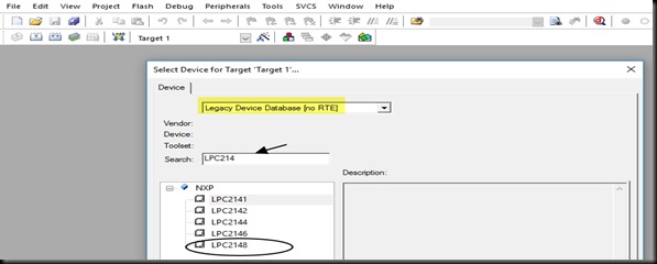
In the next window dropdown select Legacy Device & search for LPC2148.
Select the IC LPC2148 .
If LPC is not listed then check the legacy support installation
Click on Yes to add STARTUP file to project.
Different manufacturers for LPC2148 use same ARM CORE. So STARTUP file is required which initializes ARM Core Peripherals , define stack program , Interrupt vectors ,etc..
START UP file will be in ASSEMBLY language only & must be part of your program which takes care of HARDWARE INITIALIZATION.
Now the PROJECT is created
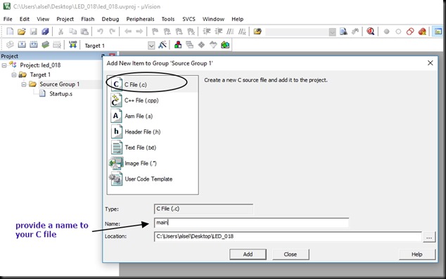
Right click on SOURCE GROUP 1 & click “Add New item to Group Source Group 1”
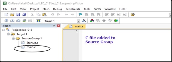
Select C File & provide a name to your C file (without .c extension .Its added automatically)
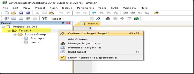
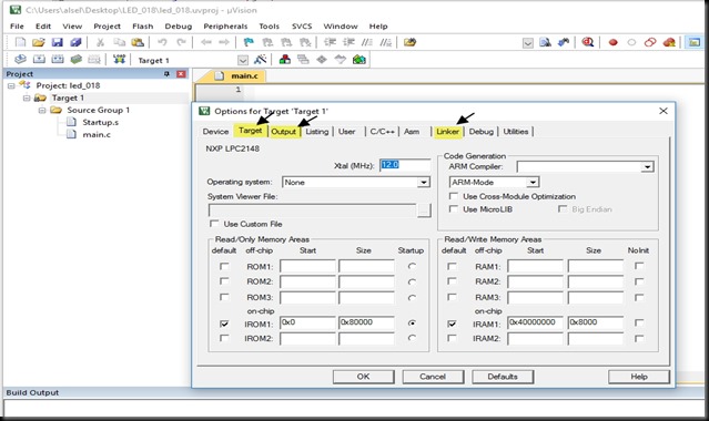
Right click on TARGET1 & select OPTIONS FOR TARGET TARGET 1
3 important settings to be done , before starting your C code.
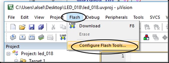
The Options for TARGET can also be accessed from FLASH –> CONFIGURE FLASH TOOLS
Following 3 settings to be done for proper compiing.
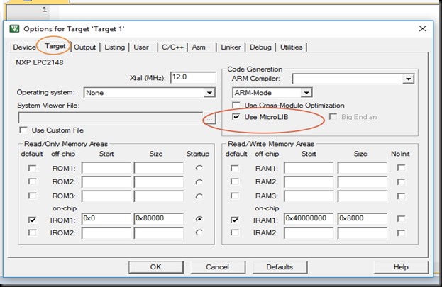
Under TARGET tab select “Use MICROLIB”
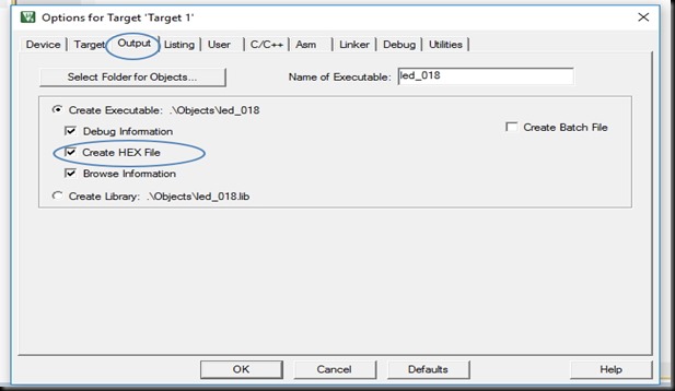
Under OUTPUT tab select CREATE HEX FILE
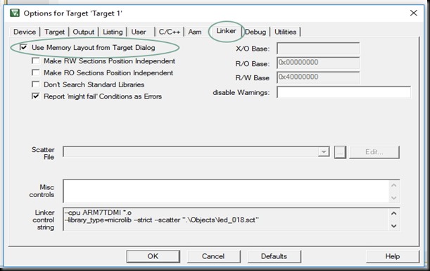
Under LINKER tab select “ USE MEMORY LAYOUT FROM TARGET DIALOG”
If the LINKER setting is not done , your C code will compile to HEX file .But on uploading you will not see any result.
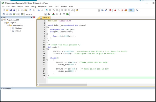
Now click on your .c file under Source Group & type in the following code :
———————
#include <lpc214x.h>
void delay_ms(unsigned int count)
{
unsigned int i=0,j=0;
for(i=0;i<count;i++)
{
for(j=0;j<3000;j++);
}
}
/* start the main program */
int main()
{
PINSEL1 = 0x000000; //Configure the P1 Pins for GPIO;
IODIR 0= (1<<18); //Configure the P0.18 pin as OUTPUT;
while(1)
{
IOSET0 |= (1<<18); //Make p0.18 pin as high
delay_ms(1000);
IOCLR0 |= (1<<18); // Make p0.18 pin as low
delay_ms(1000);
}
}
——————————-
The C code starts with inclusion of 2148 header file
#include <lpc214x.h>
Next is the DELAY function which accepts an integer parameter count & creates delay
void delay_ms(unsigned int count)
{
unsigned int i=0,j=0;
for(i=0;i<count;i++)
{
for(j=0;j<3000;j++);
}
Then starts the MAIN program
In LPC2148 each pin can perform 4 functions which is decided by setting PINSEL Register
Lpc2148 have two General Purpose I/O ports PORT0 & PORT1 ( both are 32-bit bi-directional ports).
In PORT0 P0.24, P0.26, P0.27 are not available for user & P0.31 is available for digital output only.
In PORT1 P1.0 to P1.15 is not available physically. Only P1.16 to P1.31 is available.
So out of 64 pins 45 pins are available for user
& these pins can perform multi functions decided by PINSEL Registers.
There are 3 such registers
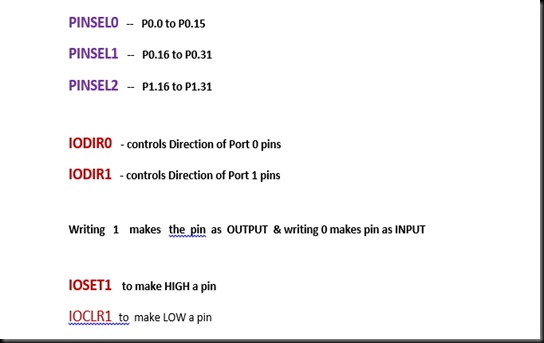
PINSEL0 controls P0.0 to P0.15
PINSEL1 controls P0.16 to P0.31
PINSEL2 controls P1.16 to P1.31
PINSEL is 32 bit register , Each pin is allotted 2 bits so 16 x 2 = 32 , each PINSEL controls 16 pins
Check out the following table

For e.g take P0.1 , the position of the pin is bits 2 & 3 of PINSEL0
If these bits are 00 then P0.1 will perform as GPIO
If the bits are 01 , P0.1 will perform as RxD
If the bits are 10 , P0.1 will perform as PWM3
& if the bits are 11 , P0.1 will perform as EINT0
So if you want P0.1 as RxD , make the bits 2 & 3 as 01
0 0 0 0 0 0 0 0 0 0 0 0 0 0 0 0 0 0 0 0 0 0 0 0 0 0 0 0 0 1 0 0
PINSEL0 = 0X000000004; is the code that makes it
By default , all pins perform as GPIO .Even if you do not define PINSEL , the pins will perform as GPIO.
But it’s a good coding practice to define PINSEL
In our code we use P0.18 to connect with an LED .P0.18 falls under PINSEL1
PINSEL1 = 0x000000; //Configure the P1 Pins for GPIO;
Next we need to define the DIRECTION of the GPIO pin .2 Registers are available to control the Direction
IODIR0 – for PORT0 pins
IODIR1 – for PORT1 pins
Writing 1 makes the pin as OUTPUT
writing 0 makes the GPIO as INPUT
To make P0.18 as OUTPUT write 1 at 18th bit
so IODIR0 = 0X00040000; makes P0.18 as OUTPUT
We can also use the BIIT OPERATOR ,
LEFT SHIFT binary 1 18 times makes P0.18 as OUTPUT
IODIR 0 |= (1<<18); //Configure the P0.18 pin as OUTPUT
Always use |= operator , which makes other bits unaffected
You can follow any method bit operator or Hex notation.
Next is the never ending loop , inside which we make the P0.18 as HIGH & after a delay make it LOW
thus blinking the LED connected to it.
while(1)
{
IOSET0 |= (1<<18); //Make p0.18 pin as high
delay_ms(1000);
IOCLR0 |= (1<<18); // Make p0.18 pin as low
delay_ms(1000);
}
2 Registers are used for this IOSET & IOCLR
Writing 1 to IOSET register makes the pin HIGH
Writing 1 to IOCLR register makes the pin LOW
Writing 0 to these registers have no effect.
Save the code by clicking the SAVE icon
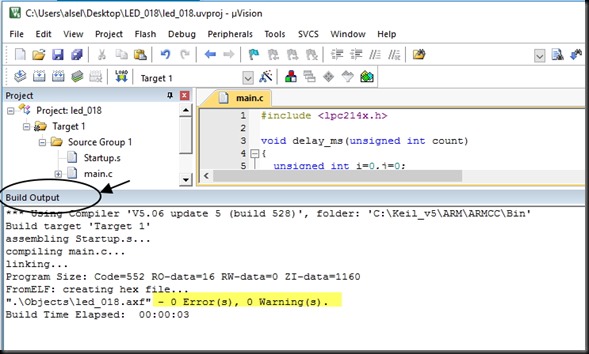
Click build icon or F7 button to build the project.
If the code is perfect you get 0 errors & 0 warnings
Now the HEX file is created .
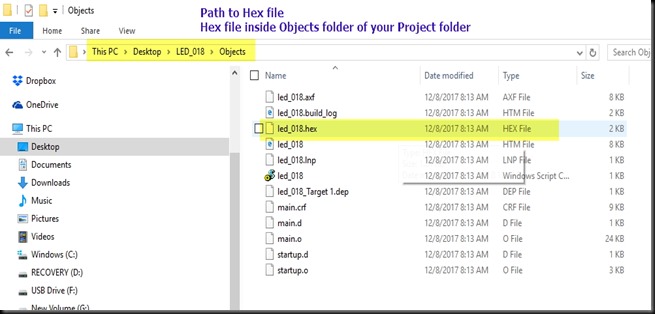
Note the path of the HEX file , it is under your project folder –> OBJECTS
There are 2 applications to upload the HEX file on to the LPC2148
FLASH MAGIC & PHILIPS 2000 UTILITY
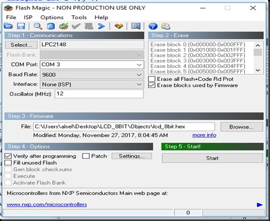
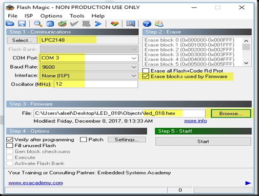
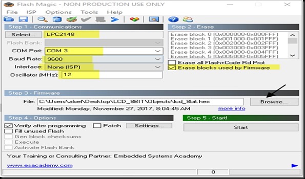
Open the FLASH MAGIC application
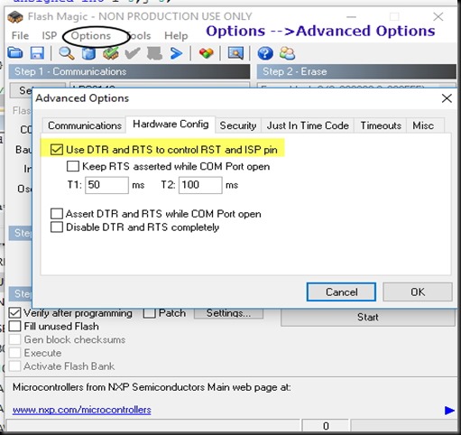
Click on OPTIONS & put a tick mark against “ USE DTR & RTS
Select the IC as LPC2148
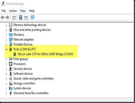
COM port is the one allotted under Device Manager.
Baud Rate is 9600 & Interface is ISP
Click on BROWSE & navigate to the location of the HEX file (under OBJECTs Folder)
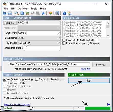
Select the HEX file & click START button to UPLOAD the HEX on to LPC2148.
Note that I’m using a development board with USB upload facility (CP2102 built in).Otherwise you need to press the ISP & RESET buttons together for uploading the HEX file.
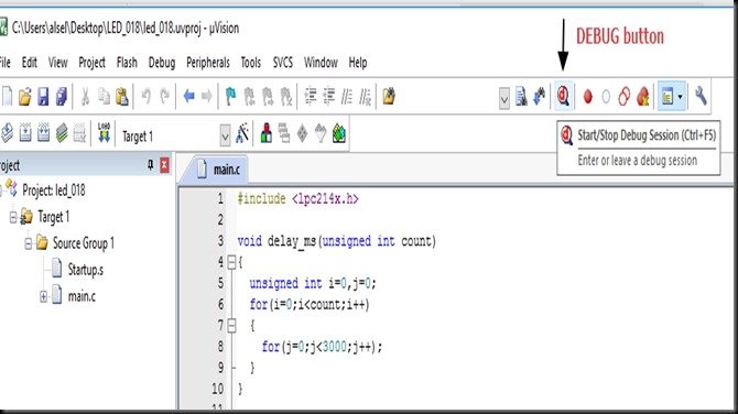
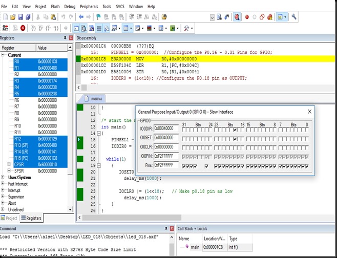
There is also DEBUG facility in KEIL.
Click on DEBUG icon to start debugging.
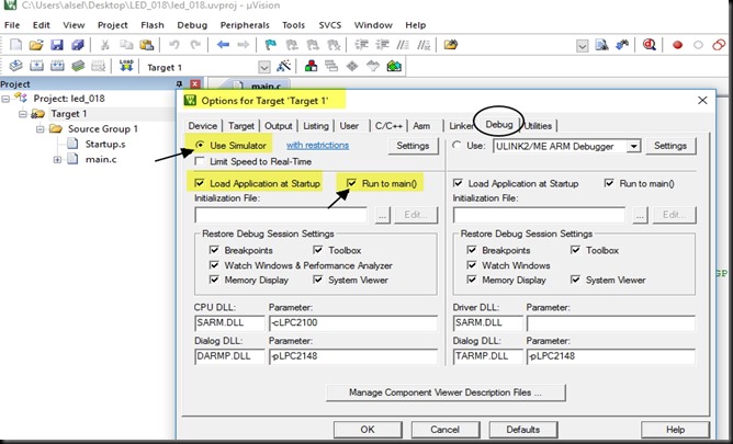
Under OPTIONS for Target , go to DEBUG tab & select
USE SIMULATOR
LOAD APPLICATION ON STARTUP
RUN TO MAIN
Under VIEW you can select the PORT0 to see the OUTPUT
VIDEO TUTORIALS :

