Latest Entries »

DWIN HMI Touch Displays can be used as MODBUS RS485 MASTER.

PYMODSLAVE simulator software is used in this demo as Modbus slave.

Modbus is protocol and RS485 is physical electrical media for data transmission. It is industry standard and can run up to maximum 1000 meters length. Compared to RS232 it is less prone to noise.

In this demo we have 3 background images. Note the naming of images start from 00.jpg.

DWIN Display used here is 5-inch 800 x 480 resolution capacitive touch model. Background images are matched to this resolution. Using ICL tool we first create 32.icl file for background images and save it inside DWIN_SET folder of the project.

In the first image 00.jpg we define some VP address locations for Analog Input and Analog Output values.

The Modbus command to Read Analog Input is 0x04. We define 3 locations as DATA VARIABLES with VP address 2000, 2001 & 2002.

For Reading Holding Registers AO , command is 0x03 and 2 VP address as DATA VARIABLES 2200 & 2201.

To WRITE Single Holding Register AO , command is 0x06 and we use data variable with VP 2500.

A keyboard pop up is used to feed in the value.

For writing to multiple registers , the command is 0x10 and VP address we use 2600, 2601 & 2602 , all contiguous.

For keyboard pop up we use VARIABLE INPUT from Touch Control menu over the Data varibale.

The VP address for Data INput must be same as that of Data Variabel.

For command 0x06 the VP used is 2500.

For command 0x10 VP used is 2600, 2601 & 2602.

Page 3 is 02.jpg and here we have a KEYBOARD .The elements of keyboard are defined using BASIC TOUCH module and respective key code HEX values are provided.For e.g no. 1 hex value is 0x0031, 2 is 0x0032 , etc as given in the note below.

Here is the KEYBOARD pop up configuration.

VP address is same as Data variable.

Data uploading is Enabled. Variable type is INTEGER 8 digits.

Font ID is 0 and font size is set to 20.

Cursor color is set to White. Display method is Direct Display , which means we can see what we type.

Keyboard location is set to OTHER PAGE.

Now click on Keyboard setting. Select the 02.jpg image where we have configured keyboard.

Select the area of display of Keyboard and click OK.

Now you can see the page id as 2 and keyboard area coordinates..

Against Show location click on SET.

Click on any area of image .This is to select the coordinate for left top area of keyboard. click OK.

Now the Show location coordinates are set.

Enable limits is optional. If required you can provide the minimum and maximum values that keyboard can input.

Scroll up to another show location on top and click SET.

Enable the Display Keyboard.

Keyboard is displayed on screen. Now click a dot on the keyboard area where numbers will be displayed.

Save the project.

Under Display , click on Preview from Current page.

You can preview your project. Click on AO 0x06 command location. A keyboard pops up. Feed in some value, which appears at the VP location.

Double click preview window border to close preview.

Same way you can implement keyboard pop up for VP 2600, 2601 & 2602.

Copy and paste the Data input over the new VP and just change the VP address.

Next page is 01.jpg.Here we define VP address locations for slave 3.

To READ DISCRETE Output Coil command is 0x01.

Read Discrete Input Contact 0x02

Write Single Discrete Coil is 0x05. Write Multiple Coils command is not yet implemented in DWIN.

VP address locations to be defined as per BIT AREA 1 and 2 .

As Read and Write Coils are BIT oriented ( 1 AND 0) , DWIN has 2 BIT areas.

AREA 1 is from 0x100 to 0x10F

AREA 2 is from 0x110 TO 0X11F.

And we have to provide the command in 22_Config.bin file atarting location 0x1C000.

The VP address location to be used in config file is as per table below.

For e.g AREA 1 , if we use VP as 0x101 , then we have to use vp as 0010 in config file.

Now in page 2, 01.jpg we will define the VP address locations as per table .

For Reading Discrete Output Coil we use BIT ICONs.

VP address we use from AREA 1 , 0X101.

Under Biticon ON OFF click on SETTING.

Select the BIT POSITION.

FOR FIRST ICON BIT POSITION SELECTED IS 0.

Icon file is selected as 42.icl.

ICON0S and ICON1S are used.

Click on the + symbol.

Select the icon for 0S and then for 1S. (OFF icon and ON icon).

Same way select the bit 1 for next bit icon

Bit 2 for the 3rd , Bit3 for the 4th biticon.VP remains the same 0x101.

For Reading Discrete input contact we use BITICON and now we use VP 0X102 from AREA 1.

Bit settings done for bit 0 and bit 1.

For Writing Single Discrete Coil , we must use VP from AREA 2..

Bit ICON is used and VP we select from AREA 2 as 0X110.

Bit setting is done as 0, 1 and 2 for the 3 Bit icons.

As we have to Write to Slave we implement Incremental Adjustment over these 3 Bit icons for Write Coil.

Incremental ADj VP is same as Bit icon 0x0110.

Respective BIT position is selected as 0, 1 & 2.

Adjustment method is ++.

Overlimit operation is Cycle , Adj step length is 1.

Lower limit 0 and upper limit 1.

Click save project and then GENERATE.

Inside DWIN_SET folder you can see the .bin files generated.

Add 0.HZK file for fonts.

Most important is the OS bin file. From official website download the Kernel files for MODBUS Master.

Download link here

Select the correct bin file.Here we use baud rate 9600 and our 5 inch model supports RS485 at UART5.

So we have copied and pasted the correct OS bin file.

SAS

0.HZK font file can be generated from under the Welcome screen.

The 22_Config file to be copied and pasted outside DWIN_SET folder.This file has to be modified for commands at location starting 0x1C000 and placed back to DWIN_SET folder .Finally this DWIN_SET folder is downloaded to DWIN HMI using SD card method.

To edit 22_Config file , we use PSPAD Hex editor.

http://www.pspad.com/en/download.php

open the 22_Config.bin file with PSPAD Hex editor and go to location 0x1C000

where the Modbus instruction command starts.

The first command is

5A02 0403 5001 0000 2000 0064

D0 D1 D2 D3 D4 D5 D6 D7 D8 D9 D10 D11

D0 : 5A Execute this Instruction
D1 : SLAVE ID (here it is 02)
D2 : Command 0x01,0x02,0x03,0x04,0x05,0x06,0x10 (04 is used here)
D3: Length of Data in word (03 means 3 word or VP address locations)
D4 : Receive Time out 2 -255 msec ( 50 msec used here)

D5 : Command Execute Mode 00 – 04 ( 01 mode means , next 2 bytes mention the page id)
0x00=Execute unconditionally.
0x01=Execute under the page specified by D6.D7.
0x02=Execute when the key value specified by D6.D7 is non-zero,
and the key value will be cleared after the command is executed.
0X03=In the 0x06 command, when the value of the variable
pointed to by D 8 .D 9 is non-zero, it will be sent automatically.

D6.D7: When D5=00, no configuration is required.
When D5=01, the configuration is page number (0002).
When D5=02, it is configured as the key address for trigger sending.
When D5=03, no configuration is required.
When D5=04, no configuration is required.0

D8.D9: This command operates the source variable address ( VP 2000 used here)
or starting address ( 1000H) allocated in the DGUS screen .
D10.D11: The slave address point table (0x0064 = decimal 100 ) operated by this instruction.
D12.D13.D14.D15: Undefined.

The second instruction is

5A02 0302 5001 0000 2000 006E

5A is start instruction and 02 is SLAVE ID.

03 is command to READ HOLDING Registers , following 02 means 2 words or 2 VP address locations

50 is 50 msec timeout

00 is mode , which means applicable on all pages .Following 2 bytes are 0000 when mode is 00.

2000 is the starting VP address

006E is slave address decimal equal to 110.

Copy this 22_Config.bin file and paste it to DWIN_SET folder.

Already we have stored the correct OS file for 9600 baud UART5 Modbus Master.

Save this DWIN_SET folder to the SD card.Note that maximum 16GB card is supported and it has to be formatted as FAT32 file system and allocation units 4096 bytes.

Plug the SD card on to DWIN and power on.

Blue download screen appears.

When download is completed , remove power and then remove SD card.

Now if you power up DWIN , you can see the project images on screen.

Next we shall connect the display to PC using an USB-RS485 converter. A B pins of DWIN is configured for RS485 communication at baud 9600.

The RS485-USB device used here is built on CP2102 driver.On connecting to PC a COM port is allotted.Here it is COM8 .Note it down.

pyModSlave software is downloaded from link :

https://sourceforge.net/projects/pymodslave/files/latest/download

Open the pyModSlave software .Click options –> Modbus RTU

Set the serial port as COM8 , as that of USB-RS485 and baud rate 9600.

Slave address is set to 2 and Start address 100 (hex 0x064) which is used in the instruction command in 22_Config.bin file.

Click Connect.

Select AI Input Registers & Type in some values at address 100, 101 ,102.

These values appear on the DWIN display at the VP address as per the instruction command.

Now select AO – Holding Registers and type in some values at address 110, 111.

These values appear at DWIN VP locations.

Next is the command instruction to write Holding Registers.

For this , instruction command to be stored in 22_Config.bin file

5A02 0601 5000 0000 2500 0078

5A02 1003 5000 0000 2600 0082

06 is the command to Write Single Holding Register.

10 is the command to Write Multiple Holding Registers.

Include this 22.bin file within DWIN_SET folder and download it to hardware.

From DWIN display touch on the Write single Register VP location. A Keyboard pops up as per design.

Feed in some value.

Same way feed in some values at Multiple Write VP locations.

On PyMod slave select AO Holding Registers.

At decimal address location 120 and 130 you can see the values entered on DWIN.

Next we shall feed in the command instructions for page 2 .We will use SLAVE ID 3.

DD

dd

FF

EE

SS

DD

SS

SS

SS

AA

SS

DD

DD

SS

DD

AA

DWIN HMI display can be configured to be used as a MODBUS Slave. Step by Step configuring is explained in this post.

To start with, collect the background images that matches the resolution of your hardware. Here we have a 5-inch industrial grade display of 800 x 480 resolution. It has A B pins at UART5 , where we implement RS485. Power source required is 12v 2 amp.

A RS485-USB device is needed for Modbus communication. A is connected to A of DWIN and B to B.

A com port is allotted to this device through which communication happens.

From the official website, download the MODBUS SLAVE files. Select the one that matches your requirements. We are using here 115200 baud, UART 5 file. Select the OS bin file and paste it inside the DWIN_SET project folder.

https://www.dwin-global.com/uploads/Slave1.zip

We have 3 background images in this project.Note the naming of images starts from 0.

0 page is for testing READ commands from Master.Commands tested are

0x03 Holding Register

0x04 Input Registers

Page 1 is for testing WRITE Commands from Master.

0x06 Single Register

0x10 Multiple Registers

Coils Read/Write can be tested only from a physical PLC Master and not from a simulator software.

page 2 has a keyboard. Here we implement Basic Touch over the keys with Hex values. Pop up keyboard implementation you can refer our previous video here :

Back ground images in folder 32

Icons in folder 42.

You need to generate .ICL files for images and icons using the ICL tool and save as 32.icl & 42.icl under DWIN_SET folder.

Inside DWIN_SET folder you have the .icl files, UART5 bin OS file and the .HZK file for fonts.

In the first page of design we have a background image 0.jpg.

From ICON display , BIT ICON is selected and we provide a VP address 0x1100 .

Bit icon setting enabled for LSB bit.

ICON0S & ICON1S selected from 42.icl for OFF and ON icons.

For Touch effect we use INCREMENTAL ADJ over the BIT ICON and the VP must be same 1100.

Bit number is set as 0.

Adjustment method ++ ,

step length : 1, Lower limit : 0, Upper limit : 1, Touch effect : Disposable

Next we add a Data Variable with VP 1200. Variable type as Integer 2 bytes.

Over this we add a Data Input from Touch and configure the pop up keyboard. VP is same as Data variable 0x1200.

Pop up key board is in image 2.jpg.

Using Basic Touch all digits are configured with respective Hex values.

For testing 0x04 command Input Registers we use 3 Data varibles with contiguous VP address starting 0x1300 , 1301 & 1302.

For Data input using pop up keyboard we implement Data Input from touch over these 3 Data varible locations.

Finally in the image 01.jpg for WRITE Commands from Master , we use Data variable with VP address 2000 and a Variable icon with VP 2050.

This is to test 0x06 Write Single Register from Master.

QMODMASTER freeware open source is used as Master Simulator :

https://sourceforge.net/projects/qmodmaster/

Open QMODMASTER software Master simulator.

Click on Options –> Modbus RTU

Select the COM port allotted to the RS485-USB device.

Baud Rate is 115200 ,as we have downloaded the 115200 OS to DWIN.

Data bits 8 , No Parity , 1 Stop bit.

From Options –> Settings

Ensure that Base Address is 0

Response timeout minimum 1 sec and Big Endian.

Modbus Mode is RTU , Slave Address is 1 , Scan Rate is 1000 msec.

Select from drop down , the Function Code as 0x03 which is for READ HOLDING REGISTERS.

VP address is 1100 HEX.

As this Master software allows address entry in HEX , it is easier to enter the VP address of DWIN directly.

Set the Number of Registers to 1 , as we Read from one Register address of DWIN 0x1100.

From Commands click on CONNECT to establish MODBUS communication.

From DWIN touch the vp location 1100 to ON icon.

You must click Commands –> Read/Write to execute.

Now you can see the ON value 1 .

Now change the icon back to OFF on DWIN.

Click Read/Write Command.

The data changes to 0.

Next , change the START ADDRESS to 0x1200

Function code is 0x03.

From Dwin touch on the vp location 0x1200. A keyboard pops up , as per the project design.

Key in any data value and press ok.

On QMODMASTER click Read/Write command to see the value set at vp 1200.

At VP location starting 0x1300 we have 3 Data variable locations in DWIN.

Feed in some decimal values using the pop up keyboard.

In Master , set the Function code as 0x04 READ INPUT REGISTERS.

Start address as 0x1300 and number of Registers as 4.

Click Read/Write command to get the values from DWIN .

Next set the Function code as 0x06 WRITE SINGLE REGISTER.

VP as 0x2000.

Feed in a value at this single register in Master.

Click Read/Write.

The decimal data from Master will appear at DWIN vp address 0x2000.

Change address to 0x2050 and feed in a value 1.

Click Read/Write to see the icon change from OFF to ON at VP 0x2050.

Change the address to 0x2100 and set the number of Registers to 3.

Feed in some values at this 3 register locations of Master.

Click Read/Write to get the data on DWIN Slave.

Video Demo :

https://www.alselectro.in/copy-of-raspberry-pi-displays

The BTS7960 is a high-current full-bridge motor driver module. The Key features are:

  • Input voltage: 6V to 27V
  • Maximum allowable current: 43 A
  • PWM capability: up to 25 kHz
  • Two PWM output pins for speed control in direct and reverse directions
  • Two EN output pins to control motors
  • Two IS input pins to protect against high current and heat

BTS7960 is a fully integrated high current half bridge for motor drive applications.
This contains one P- channel high side MOSFET and one N channel low side MOSFET with
an integrated driver IC in one package.

This module can be used to drive  2 wire huge current Motors .Not suitable for Stepper Motors .

In this post we will be using a huge current Motor 24v 250Watts like this :

A separate power source is required for this Motor.

24v 10Amp Metal SMPS is used for this source

This module has 12 pins:

Microcontroller pins (Low current):

  • VCC: Module power supply – 5V
  • GND: Ground
  • IS-R: Input signal for detecting high current – Straight rotation
  • IS-L: Input signal for detecting high current – Inverse rotation
  • EN-R: PWM Signal for controlling motor speed – Straight rotation
  • EN-L: PWM Signal for controlling motor speed – Inverse rotation
  • PWM-R: for controlling motor RIGHT direction
  • PWM-L:  for controlling motor LEFT direction. 

Motor pins (High current):

  • M+: Motor Positive
  • M-: Motor negative
  • B+: Battery positive
  • B+: Battery negative
  • You cannot overload the BTN7960B to destruction. It will overheat and safely shut off. Then restart when it cools and the Enable line is pulsed low then high . Under voltage Shut Down: To avoid uncontrolled motion of the driven motor at low voltages the device shuts off . If the Supply voltage  drops below 5.4V , The Motor driver will switched Off , And won’t turned on untill the Supply voltage increased to 5.5V Or more .
  •  Over temperature Protection: The BTS 7960 is protected against over temperature by an integrated temperature sensor. Over temperature leads to a shut down of both output stages.
  • Current Limitation : The current in the bridge is measured in both switches, High and Low side.If the current reaching the limit current  the switch is deactivated and the other switch is activated for a certain time.
  • To get the Motor to move in an H-bridge the Enable inputs should be held high and PWM-A and PWM-B should be different polarity.
  • Don’t pulse the enables and hold the PWM inputs at a DC level. Some old driver chips can do this. The BTN7960B doesn’t work that way.
  • The naming convention is bit confusing.
  • R PWM & L PWM pins can be pulled HIGH or LOW to enable Direction of Rotation.
  • R-EN  & L-EN pins are used for speed control using PWM.Generally , these 2 pins are connected together to a PWM pin of Arduino. AnalogWrite command is used to control speed.

Connect the Motor red wire to M+ and black wire to M-.

Connect B+ of module to positive of 24v 10amp power source . B- to negative of SMPS.

Make use of thick copper wires for power connection as the motor takes high current.

The module has  8 control pins.

Vcc is connected to 5v of Arduino & Gnd to Gnd of Arduino.

R_IS & L_IS are for current limit alarm outputs, which are not used in this demo.

R_EN & L_EN ins are Right,Left speed control pins .Both are connected together to D11 of Arduino. Note that we use a PWM enabled pin of Arduino for this.

L_PWM is connected to D10 ,  R_PWM is connected to D9. These 2 pins decide the direction control of the motor.

Now upload the following code to Arduino.

To run the motor in CW direction we make R_PWM pin High and L_PWM pin Low.

To make the motor run in CCW –   R_PWM pin Low and L_PWM pin HIGH.

To stop the motor both pins are made LOW.

Speed is controlled using ANALOGWRITE function where the PWM pin is given a value from 0 to 255.

——————–

#define RPWM 9
#define LPWM 10
#define PWM 11

void motor_cw(){              //CLOCK WISE
  digitalWrite (LPWM, LOW);
  digitalWrite (RPWM, HIGH);
  analogWrite (PWM, 255); // 0- 255  
  Serial.println (“MOTOR RUNS CW”);
  }
void motor_ccw(){              //ANTI CLOCK WISE
  digitalWrite (LPWM, HIGH);
  digitalWrite (RPWM, LOW);
  analogWrite (PWM, 255);
  Serial.println (“MOTOR RUNS CCW”);
  }

void motor_stop(){          //motor stop
  digitalWrite (LPWM, LOW);
  digitalWrite (RPWM, LOW);
  analogWrite (PWM, 0);
  Serial.println (“STOP”);
  }
 
void setup() {
Serial.begin(9600);
Serial.println(“START”);
pinMode (RPWM, OUTPUT);
pinMode (PWM, OUTPUT);
pinMode (LPWM, OUTPUT);
}

void loop()
{
delay(2000);
motor_cw();

delay(5000);
motor_stop();

delay(5000);
motor_ccw();
}


The HM-10 BLE Wireless Module-Original is a readily available Bluetooth 4.0 module, which can configure as either Master or slave.

This module is used for establishing wireless data communication. The module is designed by using the Texas Instruments CC2541 Bluetooth low energy(BLE) System on Chip (SoC). You can use it simply for a serial port replacement to establish connection between MCU & your embedded project

It is fully configurable by a rich and well documented AT command-set and allows transparent data communication via serial UART (default baud rate 9600 bps).

The Bluetooth 4.0 HM-10 is basically a breakout board for cc2541, it broke out the LED pins, RX/TX and also adding the voltage regulator that regular 5v to 3.3 v.

Clones available in market have on board only single crystal and the Firmware of clones support limited AT commands.Clones are mostly named as  MLT-BT05

Image 12

Pin Description:

  • STATE: state test pins, connected to an internal LED, generally keep it unconnected.
  • BRK: break connect, it means breaking the Bluetooth connection, generally keep it unconnected.
  • VCC: positive pole of the power source.
  • GND: Ground.
  • TXD: serial interface, transmitting terminal.
  • RXD: serial interface, receiving terminal.
    For testing AT Commands we need an USB-TTL module built on CP2102 ic.
    Connection between HM10 and USB-TTL is shown below :

Image 3

Tx of HM10 can be connected directly to Rx of USB-TTL.

Rx of HM10 to be connected through a level shifter to Tx of USB-TTL. A 1k in series and 2k2 across to Gnd is a simple level shifter.

HM10 can be supplied power 5v , as there is on board 3.3v regulator.

Connect the USB –TTL to PC and note the COM port allotted.

Image 1

We require a TERMINAL software to test AT commands.

The HM10 module do not wait for a Carriage Return .So Putty terminal cannot be used.We use COOLTERM terminal in LINE MODE.

https://freeware.the-meiers.org/CoolTermWin.zip

Install COOLTERM software.

Open OPTIONS

Under Serial port select the COM port of USB-TTL , Baud Rate 9600, 8N1

Image 4

Under TERMINAL setting select LINE MODE.

This allows sending AT commands as a single packet.

Image 3

Click on CONNECT.

Typing AT on the line mode gets an OK reply from HM10.

Image 5

To get the MAC address of HM10

AT+ADDR?

Image 6

Notice the usage of ? for a Query command.

For assignment we do not use =

Just feed in the value after AT command.

For e.g to change the password from default 000000

AT+PASS123456

After PASS we do not use = symbol.Just provide the value.

Image 11

AT+NAME?

Returns the default name of the module as HMSoft.

To change name AT+NAMEmyHM10

ROLE of HM10 by default is SLAVE.

To change to MASTER mode

AT+ROLE1

On Master mode the HM10 will not broadcast its name.Pairing can be initiated only from a MASTER.

Image 7

AT+BAUD?

returns 0.

By default HM10 is in AUTO BAUD mode 0.

You need to set the baud rate by

AT+BAUD9600

AT+POWE?

Returns the transmit power of module which is o dbm by default.

To restart the module

AT+RESET

Image 8

There is an LED connected to PIO1 on board whish shows the STATUS.

Default value is 0 which makes LED blink 500ms  ON/OFF when in disconnected mode.

When paired , the LED goes ON steadily.

Image 9

Now let us pair this module from an ANDROID phone which will be Master.

Install the application BLE TERMINAL.

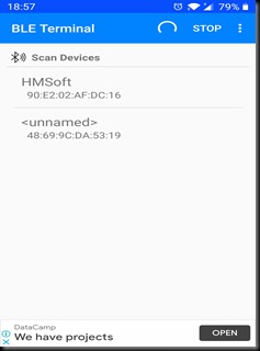
Open the application and Scan for devices.

HM10 appears as HMSoft.

2021_04_07_18.57.27                                    2021_04_07_18.57.39

Touch on this HMSoft and provide the password to pair.

2021_04_07_19.06.11                    2021_04_07_19.06.18

Once paired the LED on HM10 glows steadily.

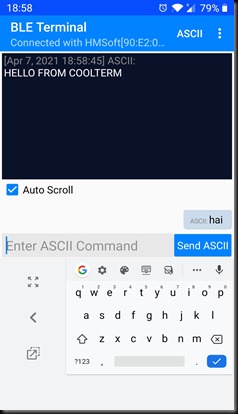
Now you can type some characters on phone which is received at HM10 Coolterm.

From Coolterm window you can type and receive on phone BLE Terminal.

2021_04_07_18.58.49

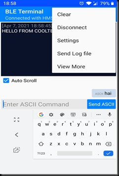
To DISCONNECT you can touch on the disconnect.

2021_04_07_18.58.56

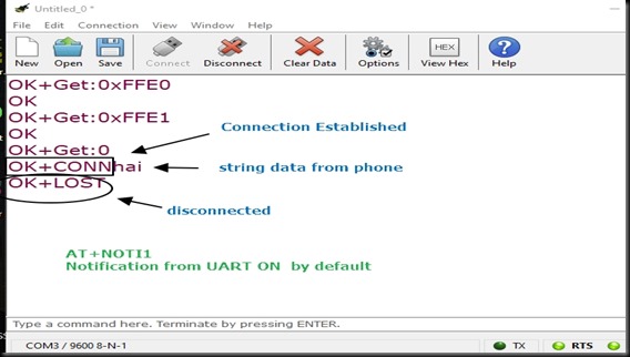
At the COOLTERM you get the NOTIFICATION.

Image 10

VIDEO TUTORIALS :

blog_image

ESP32-CAM is a camera module based on ESP32. It comes with an OV2640 2 MP camera and provides onboard SD memory card slot.

It is suitable for home smart devices,  wireless monitoring, and other IoT applications.

ESP32 CAM module has on board PSRAM.

Image 2

The OV2640 camera module on the ESP32 Camera board can support a max resolution of 1600 x 1200 pixels, however without PSRAM the camera frame buffer can only support a max resolution of 800×600 pixels

Boards with PSRAM (typically 4MB) can support the max resolution and also support 2 concurrent frame buffers. This provides for a better streaming experience as while  one frame is being sent , the camera is working on capturing the next frame.

PSRAM

Always Power up the module using 5V .Powering the board with 5V increases stability .

Image 1

pins

The camera module has no USB input.So we need a FTDI programmer or USB-TTL module to upload program.In this testing we make use of an USB-TTL module built on CP2102 IC.

Connection between ESP CAM & USB-TTL is simple.

We make use of the 5v power from USB module itself.

Gnd is connected to Gnd pin of Camera module.

Rx of USB module to Tx (printed as UOT) of Camera module.

Tx of USB module to Rx (printed as UOR) of ESP CAM.

c1

Do not use 3.3 V AS POWER SOURCE .

For PROGRAM Mode the GPIO0 pin must be connected to GND.

Plug in the USB-TTL module to PC and note the COM port allotted under Device Manager.

Image 1

To use Arduino IDE for programming , we need to install the ESP32 boards Manager for Arduino.

From Arduino IDE open File—> Preferences

Image 2

Copy and paste the following json link for additional Boards Manager :

https://raw.githubusercontent.com/espressif/arduino-esp32/gh-pages/package_esp32_index.json

click OK to close the window.

Image 4

Click   Tools  –> Boards –> Boards Manager

Image 5

A separate window opens.

Search for ESP32 and install the latest version.

Image 6

Once the ESP32 Board package is installed , you can select the ESP CAM board under Tools.

Click Tools  –> Board –> ESP32 Arduino

and select AI Thinker ESP32 CAM

Image 7

And then select the COM port.

Image 8

Now open the File –> Examples –> ESP32 –> Camera  –> Camera WebServer

Image 9

It is a sophisticated program.

To start with you need to select camera model .

For this , uncomment CAMERA_MODEL_AI_THINKER and comment all other:

Then enter SSID and PASSWORD for your WiFi router.

Image 10

Click on UPLOAD.

If GPIO0 is not connected to GND , you get a fatal error.

Image 11

Ensure that GPIO0 is connected to GND and click Upload.

While you see Connecting…….. at the bottom of IDE , Press the RESET switch on CAM module.

Image 13

RESET switch has to be pressed at the right time while you see Connecting…….

reset

If RESET is not pressed properly , you get Error : Failed to Connect

Image 14

Image 16

Image 18

Once uploading is successful you see the message

Leaving….

Hard Resetting via RTS pin…

Image 20

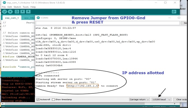
Now open the SERIAL monitor of IDE.

Remove the GPIO-GND Jumper.

and press the RESET switch.

WiFi connected message is displayed  and you get an IP address for your Camera module.

This IP address is Dynamic and provided by your Router.

Image 21

Open the WEB Browser and type in the IP address.

Now you can see the DASHBOARD control of Camera.

Image 22

From here you can click on GET STILL button to take pictures.

Quality & Resolution of the picture can be modified by sliding the control bar provided.

Image 23

START STREAM button is provided to start streaming of live video.

Image 24

While you capture Still pictures , JPG picture details are displayed on the serial monitor.

Image 25

Following are some common problems and solutions :

If your power source is not providing enough current,

you get the following error.

Image 26

Always use 5V for supply , as 3.3v often gives problem.

Image 28

Image 29

If CAMERA MODEL is wrongly selected, you get error : Detected Camera not supported.

Always uncomment the correct model in the code and all others must be commented out.

Image 27

VIDEO TUTORIAL :

blog_image

Raspberry Pi Pico is a low-cost, high-performance microcontroller board with flexible digital interfaces.

Other Raspberry PI boards are SBC –  Single Board Computer which requires an OS on a SD card.

But PICO is a Microcontroller like Arduino.

RPI boards do not have ANALOG inputs , PICO has 3 ANALOG inputs.

Designed on RP2040 IC (Dual-core Arm Cortex M0+ processor flexible clock running up to 133 MHz)

, this PICO board has 26 GPIO pins including 3 Analog Inputs.

As such RP2040 HAS 30 GPIO pins including 4 Analog inputs, but on board the user is offered with only 26 GPIO pins including  3 Analog Inputs.

  • 264KB of SRAM, and 2MB of on-board Flash memory
  • Castellated module allows soldering direct to carrier boards
  • USB 1.1 with device and host support
  • Low-power sleep and dormant modes
  • Drag-and-drop programming using mass storage over USB
  • 26 × multi-function GPIO pins
  • 2 × SPI, 2 × I2C, 2 × UART, 3 × 12-bit ADC, 16 × controllable PWM channels
  • Accurate clock and timer on-chip
  • Temperature sensor inbuilt
  • Accelerated floating-point libraries on-chip
  • 8 × Programmable I/O (PIO) state machines for custom peripheral support

https://www.raspberrypi.org/products/raspberry-pi-pico/

pico_pins

PICO can be programmed with C / C++ SDK or MicroPython.

In this blog, we work with MicrPython.

To start with Press & Hold the BOOTSEL button on board and connect the USB to Windows PC.

CONNECT

Release the BOOTSEL button to see PICO appear as a mass storage device RPI-RP2.

Image 1

Open the Device Manager , you see PICO under Portable Devices as RPI-RP2.

Image 2

Open the RP2 storage .

Double click on the INDEX.HTM file to visit the official PICO website.

Image 3

Image 4

Scroll down to click Getting started with MicroPython.

Image 5

https://www.raspberrypi.org/documentation/pico/getting-started/static/f70cc2e37832cde5a107f6f2af06b4bc/rp2-pico-20210205-unstable-v1.14-8-g1f800cac3.uf2

Here download the UF2 file , which is USB Flashing Format by Microsoft.

UF2 files can be opened and edited using a variety of Microsoft MakeCode editors.

To transfer a UF2 file to a microcontroller, developers plug their microcontroller into their PC’s USB drive. Their PC then recognizes the microcontroller as a FLASH DRIVE, allowing the developer to drag their UF2 file to the microcontroller and install their MakeCode program.

Image 6

Drag and Drop the UF2 file on to RPI-RP2.

Image 7

RPI-RP2 now disappears indicating Micropython installation is complete.

If you open the Device Manager , PICO appears as USB SERIAL DEVICE and a COM port is allotted.

Image 8

For GUI interface we use THONNY PYTHON.

Download and install Thonny Python

https://thonny.org/

Image 9

Open Thonny Python

Under Tools –> Options

click INTERPRETER

th1

Under Interpreter drop down select

MicroPython Raspberry Pi PICO   and select the COM port allotted to PICO.

PICO is listed only in the newer version of Thonny.

th2

Now click on the RED stop button to get the Interpreter CHEVERON 3 greater than symbol at the bottom.

You can try MicroPython commands here.

Image 10

To blink the on board LED let us start the coding under Editor.

First import PIN Class from machine module.

Functions are called modules in Micropython.

Then import sleep class from utime module for delay.

Create an led object which takes 2 parameters.First is the GPIO PIN , which is 25 where the inbuilt led is connected.

Second parameter to declare this pin as OUTPUT.

Then starts the never ending loop

while True:

After the colon you get an indentation space automatically.

This is equal to braces in Micropython.

Here we toggle the led and provide a delay of 1 second.

Image 11

Click File –> Save As

Image 12

You get 2 options to save.

Select Raspberry Pi PICO to save the file.

Image 13

Provide the filename as

main.py

Auto execution takes place only if the file name is main.py.

So it is a must to provide file name as main.py.

Image 14

Click on the green RUN button

Image 15

Now the LED on board blinks according to code.

C2[3]

To RESET the PICO back to factory condition

there is another UF2 file under Resetting Flash memory.

Download this nuke UF2 file.

Image 16

Press hold the BOOTSEL button and connect the USB to pc.

IMG_20210205_182142

Drag and drop the nuke UF2 file on to RPI-RP2 to erase flash memory back to factory condition.

There is no RESET button on PICO.

You can connect a RESET button between RUN and GND pin as shown below :

reset

video :

blog_image

The MLX90614 from Melexis is an infrared thermometer for non-contact temperature measurements. Both the IR sensitive thermopile detector chip and the signal conditioning ASIC are integrated in the same TO-39 can.

Integrated into the MLX90614 are a low noise amplifier, 17-bit ADC and powerful DSP unit thus achieving high accuracy and resolution of the thermometer.

Factory calibrated in wide temperature range: -40 to 125°C for sensor temperature and -70 to 380°C for object temperature

SMBus ( I2C based) compatible digital interface for fast temperature readings and building sensor networks.

In this project we shall use the MLX90614 with OLED & ULTRASONIC sensor.Arduino NANO is used as controller.Calibration procedure for correct object temperature reading is also explained.

IMG_20200902_112028

Before coding , we need to install the required libraries for Arduino.

Open Arduino IDE

Sketch –>  Include Library –>  Manage Libraries

Image 2

Search for MLX and select ADAFRUIT MLX90614 Library to install.

Image 3

Next search for GFX and install ADAFRUIT GFX Library , which is graphic support library for displays.

Image 1

Finally search for SSD1306 and select ADAFRUIT SSD1306 to install.

Image 4

Connection details are as shown in image below.

Ultrasonic

         TRIG –> D12

         ECHO –> D11

OLED

        SDA –> A4

        SCL –> A5

MLX SENSOR

        SDA –> A4

        SCL – A5

A mini buzzer is connected to D3.

Vcc of OLED,MLX & Ultrasonic are connected to 5v of NANO

All GND pins are made common.

If you want you can use an external power source 5V 1 AMP at Vin of NANO.

As power consumption of OLED,MLX is very low , we can source power from NANO itself.

OLED & MLX are I2C devices , so they are connected to I2C pins of NANO ( SCL & SDA).

According to I2C address , respective device can be communicated.

MLX_ULTRA

IMG_20200902_112855

CODE Explanation :

Starting with we include the libraries we installed for  MLX & OLED.

Image 1

An object named mlx is created from class Adafruit_MLX90614 from MLX library.

An object display is created from class Adafruit_SSD1306 from OLED library.Here we pass argument –1 , as there is no Reset pin in OLED.

Image 5

Variables like roomTemp, objectTemp , stemp , threshold are created as Float

Ultrasonic echoPin is defined at D11 , trigPin at D12.

The Maximum & Minimum range of Ultrasonic are initiated as Integer variables.

Ultrasonic will sense the object distance and the Temperature reading from MLX will be initiated only when the Object is in between 15 and 25 cm.

Image 8

Inside void setup()

Trigger pin of Ultrasonic is declared as OUTPUT pin , Echo as INPUT pin.

OLED display is initiated using begin() function and the I2C address of OLED is passed as argument (0x3C).

setTextColor() function is used to pass argument WHITE which enables black background for OLED.

Image 7

Inside loop() we generate a trigger pulse for Ultrasonic to generate a 40kHz burst.

The pulse reflected from object is calculated as width using pulseIn() function of Arduino.

Distance of the object is then calculated.

The object temperature in Celcius is read using MLX library function readObjectTempC()

& room temperature using function readAmbientTempC()

Initially the threshold value is set as 0.

After calibration we shall fix the correct threshold value.

Image 10

Display settings for OLED by using functions setCursor() , display()

At the bottom of OLED we display the distance of target object in cm & then the Room temperature in celcius.

If distance of object is above maximum range  ( we’ve set it as 25cm) , GET CLOSER is printed on display.

If distance of object is below minimum (15 cm) , TOO CLOSE is printed.

Image 11

If the object is between 15 and 25 cm then HOLD ON is printed.

Till readcount is 5 (5 times we take reading and Average it) disptemp() is called.

Finally the object temperature is displayed.

Image 12

If object temperature is above 37.5 celcius  , play_alert() function is called.Here we use the tone()

Image 13

Finally the compiled code is uploaded to NANO.

Image 15

OLED display shows GET CLOSER initially and the object distance is displayed at the bottom along with room temperature.

IMG_20200902_154319

If the object is near to sensor ( below 15 cm) , TOO CLOSE is displayed.

IMG_20200902_154427

If the object is between 15cm and 25 cm , HOLD ON is displayed and blinks 5 times.

Reading is taken 5 times and averaged.

IMG_20200902_154459

Forehead or Wrist is shown in front of sensor for taking reading of temperature.

The display shows 31.2 degree celcius.

Image 3

We use an oral thermometer for calibration purpose.Using this meter under tongue , it shows 98.2 Fahrenheit.

Image 4

Converting F to Celcius , it is 36.8 C

Image 5

36.8 LESS 31.2 (shown by OLED initially) = 5.6

So we need to use this value as THRESHOLD.

Image 14

Update the threshold value and then upload the code.

Now the display shows the correct temperature 36.9 C

Image 7

Video tutorial :

blog_image

7 HDMI display with capacitive touchscreen is now available with resolution 1024 x 600 pixels.

The touch panel supports up to 5 touch points. And it adopts  free-driver technology, no special requirement of drivers.

There is no need for  external power supply for the screen, it can be powered by USB port and HDMI port from Raspberry PI.

  • Operating Voltage: 5V
  • Operating Current: 160mA
  • Maximum Operating current: 1200mA  (with HDMI connection)
  • Refresh Frequency: 43Hz – 60Hz
  • Screen Resolution: 1024×600
  • Video Interface: HDMI
  • Supports Raspbian,Raspberry PI  OS ,5-points touch, driver free.

Previous models are TFT displays.TFT stands for the thin-film transistor, which is just another kind of liquid crystal display.One of the major shortcomings of using TFT is that it does not offer a good level of visibility.

This new display is IPS . In-Plane Switching

IPS panels seek to solve TFT panels’ issues of poor color reproduction and viewing angles. In this regard, IPS panels have largely succeed. Not only do they offer a higher contrast ratio (superior blacks), high color accuracy , but IPS panels also have very little color shift when changing the viewing angles.

Hence, with this technology, you can view the screen from much wider angles and sides without experiencing unwanted blurriness and grayscale.

The negative point about IPS panel is their poor response rates and lower possible refresh rates, IPS panels are generally not considered for competitive gameplay

WAVESHARE make is original

IMG_20200902_134558

On the back side left top is the HDMI connector.Below that is the micro USB socket for power and touch.This USB can be connected to one of the USB ports of RPI.

A mini slide switch is there for display ON / OFF.

IMG_20200902_134626

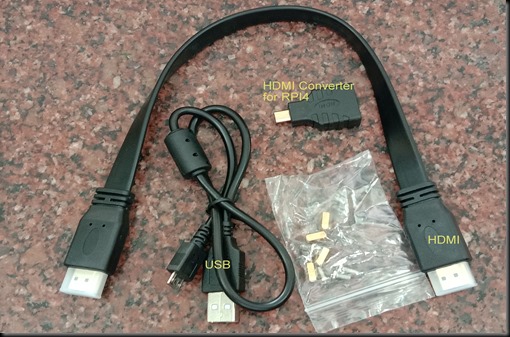
A HDMI cable , USB to micro usb cable and a HDMI micro converter ( used for RPI 4 models)

are provided with the display.

IMG_20200902_134723

Clone or Copy models similar to Waveshare are also available in the market.

Clone display has 2 micro usb sockets , one for power & the other for both power & touch.

IMG_20200830_151339

WaveShare original has EMI and ESD protection near the HDMI socket

IMG_20200902_134652

Also the original one has USB protocol translator, converting the touch signal into standard multi-points touch protocol to achieve smooth multi-points touch control.

IMG_20200902_134642

Before connecting the display to Raspberry PI , prepare the Operating System for PI.

Download the latest RASPBERRY PI OS ( previously called Raspbian) from

https://downloads.raspberrypi.org/raspios_full_armhf_latest

Use BALENO ETCHER software to write image on to SD card.Always use CLASS10 type micro SD card.

For this you need a card reader to plug SD card on to your PC.

https://github.com/balena-io/etcher/releases/download/v1.5.107/balenaEtcher-Setup-1.5.107.exe

Once the image is written on SD card , if you re plug the card reader to pc, you can see the BOOT partition . The ROOT partition is not visible on Windows machine.

Image 1

Right click on empty space and create a new TEXT document.Name it as ssh.txt

Then delete the .txt extension , so that only a file named ssh exists without any extension.

On next boot on RPI , the SSH is enabled and the file named ssh will be deleted automatically.

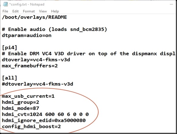
Next we need to modify the config.txt file to enable view on display.

Open config.txt file.

Image 2

Scroll to the end of file and add following commands.

Image 3

As we power the display from USB of RPI , we need to boost the current source capacity of USB port of RPI.

This is achieved by

max_usb_current=1

which makes USB current source to maximum of 1.2 amp

Setting a specific HDMI mode is done using the hdmi_group and hdmi_mode config.txt entries.

The group entry selects between CEA or DMT, and the mode selects the resolution and frame rate.

hdmi_group=2

hdmi_mode=87

To set a custom display mode we use 87 for mode.

HDMI output group is set to 2 which represents DMT (Display Monitor Timings, the standard typically used by monitors)

Then define a custom CVT  — Coordinated Video Timings

hdmi_cvt= width1024  height 600  framerate 60  aspect 6  margins 0  interlace 0 rb 0

width  1024 pixels

height 600 pixels

framerate 60 Hz

aspect 6 —  ratio  15:9

margins  0
0=margins disabled, 1=margins enabled

interlace  0
0=progressive, 1=interlaced

rb  0
0=normal, 1=reduced blanking

Setting

hdmi_ignore_edid to 0xa5000080

enables the ignoring of EDID/display data if your display does not have an accurate EDID. It requires this unusual value to ensure that it is not triggered accidentally.

HDMI_BOOST increases the amplitude and/or pre emphasis of the HDMI signal.
For long HDMI cables use value 7 or 11.

Save the CONFIG.TXT file.

Remove the SD card and plug it to RPI.

Connect HDMI cable between HDMI ports.

Connect the micro usb cable to touch port of display and the other end to one of the USB ports of RPI.

Use a power adapter of 5v and ampere more than 2 amps

IMG_20200830_151414

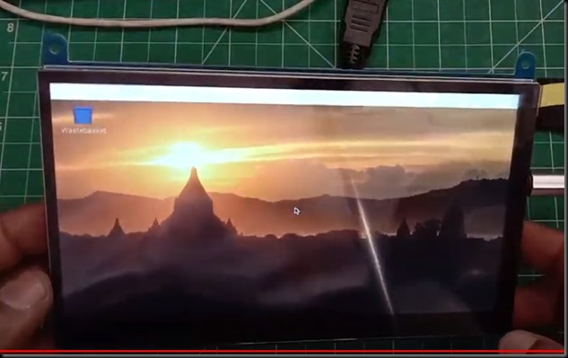
Switch on the power to see the display booting up to welcome screen of RPI.

TOUCH functions work without any installation of drivers.

Image 4

You can also set the SD card for auto connect with WIFI , and also you can install Match box keyboard for on screen keyboard.

Watch this video :

blog_image

TITLE

PIC 12F675 is 8 bit , 8 pin mini and powerful Microcontroller.

It has 1k Bytes of ROM Flash memory , 64 Bytes of RAM ,  128  Bytes of EEPROM , 4 channels of 10 bit ADC , 2 TIMERS one 8 bit and another 16 bit.A comparator and inbuilt oscillator also are provided.

This chip can be programmed using PICKIT3.

IDE used is MPLAB X and compiler is XC 8.

Connection details as below in image.

An LED is connected to pin 3 (GP4) .Short lead of LED is connected to Gnd through a Resistor 470E.

PIC3

MPLAB X IDE is the IDE used here for development.Compiler installed is XC8

https://www.microchip.com/mplabx-ide-windows-installer

https://www.microchip.com/mplabxc8windows

Image 2

Open MPLABX IDE , File  –> New Project

Select  Standalone Project

Image 3

Under Device select PIC12F675

Against TOOL , tick mark Show All and select PICKIT3 from the dropdown list.

Image 4

Next is the selection of Compiler.

Select XC8 .

If not listed , check the installation of XC8 compiler.

Image 5

Provide a Project name and browse to the location of folder created for project location.

Image 6

Now the project files are created.

Right click on SOURCE FILES and click on New –> main.c

If you want rename the file , leave the extension as .c

Click Next to add the .c file to Source files.

Image 7

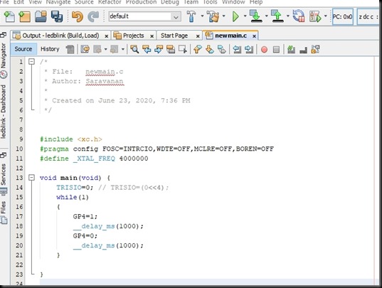
Click on .c file to see the skeleton C file.

#include <xc.h>

header file for Compiler is added automatically.

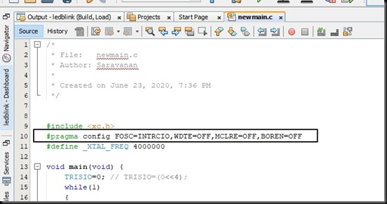
We need to set the configuration bits in the code using

#pragma config

Image 17

Settings like Internal oscillator , Watch Dog OFF , Brownout detect OFF can be

used with a comma separator in a single command line.

Image 16

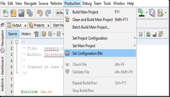
You can also verify correct settings by clicking on Production –> Set Configuration Bits

Image 9

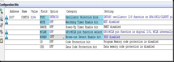
A new Window opens at the bottom.

Here you can do the needed settings and finally click on Generate code.

You can copy and paste the pragma settings inside the C code.

Or to make it simple make a single command line with comma separator.

As we cannot spare 2 GPIO pins for external crystal oscillator , most of the projects are configured for internal oscillator of 4 MHz.

This is set by

# pragma config FOSC=INTRCIO

Image 10

Next we need to define the crystal frequency

#define _XTAL_FREQ 4000000

Without this command delay function will not work.

Data Direction is set by TRISIO Register.

Making a bit 0 will make the corresponding  GPIO pin OUTPUT

and making a bit 1 will configure GPIO as INPUT.

TRISIO=(0<<4);

The above notation can also be used.Here 0 is left shifted 4 times thus making GP4 as OUTPUT.

Under never ending loop we make GP4 initially 0 and after a delay of 1 second we make it 1.

Note the usage of double underscore __ before delay.

Image 11

Before building the project , an important setting to be done to make the Power to Target from PICKIT3.

Click Set Project Configuration and then Customize.

Image 20

Select PICKIT3 and then from the dropdown select POWER.

Image 13

Put a tick mark against Power Target from PICKIT3 and click Apply.

Image 14

Now click on BUILD MAIN PROJECT or F11 Button to Compile.

Image 15

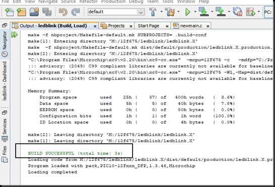
When no errors are found , you can see BUILD SUCCESSFUL.

Image 18

Now click on the DOWN Arrow icon on tool bar to upload the hex file on to chip.

Image 19

Once file is uploaded , you can see the LED connected to GP4 blinking.

IMG_20200624_162228

blog_image

ATTINY85 , a 8 bit AVR Microcontroller provides many features in lesser pins.

With program memory of 8Kbytes the controller has satisfying memory for many applications.

With various POWER SAVE modes it can work on battery operated applications.


t1

SPECIFICATIONS :

Number of  Programmable I/O pins   6           Operating Voltage  +2.7 V to +5.5V

Maximum DC Current per I/O Pin 40 mA     Maximum DC Current through VCC and GND Pins 200 mA

Communication Interface

Master/Slave SPI Serial Interface  (5,6,7  PINS)   [Can be used for programming this controller]

I2C or Two-wire Serial Interface  (5,7  PINS)  [Can be used to connect peripheral devices and sensors]

Universal Serial Interface  (5,6,7 PINS)   [Can be used for communicating with other controllers]


UART Interface   Not available        ADC Feature  4channels, 10-bit resolution ADC

Analog Comparators 1                    Timer Module   2 x  8-bit counter

PWM outputs  4                              External Oscillator   0-20MHz for ATTINY85

Internal Oscillator   0-8MHz  Calibrated Internal R-C Oscillator

CPU Speed   1 MIPS @ 1MHz

Program Memory or Flash memory size  8Kbytes

RAM size   512Bytes on Internal SRAM

EEPROM size  512Bytes of In-System Programmable EEPROM

Program Lock   Available          Watchdog Timer  Available

Power Save Modes      Three Modes  [Idle ,  ADC Noise Reduction ,  Power-down ]


Image 2


ATTINY85 can be programmed in many ways.

This post is on programming in AVR mode .

For programming we need an USBASP (also called AVRDUDE)  hardware  which is the same one used for programming 8051 ICs.


USBASP1

Connection between ATTINY85 and USBASP is by SPI pins

MOSI to MOSI (pin5)

MISO to MISO (pin 6)

SCK to  SCK (pin 7)

RST to RST (PIN 1)

Vcc to pin 8 & Gnd to pin 4 of ATTINY.

Image 3

For programming we use WINAVR (Programmers Notepad & MFILE)

usbasp driver and winavr can be downloaded from following link.

download link :

http://www.alselectro.com/files/software.zip

After installing driver for usbasp , open the Device Manager to see USBASP under libusb.


Image 1


Next install WINAVR

t2

Accept default location of installation.

Image 2

Following components must be selected

ADD Directories to PATH

Install Programmers Notepad

Image 3

Install WINAVR as ADMINISTRATOR.

Otherwise Programmers Notepad (PN) will not work.

MFile which makes RULE for programming also installed automatically.

Image 4

In WIN 8 / 10 you need to replace msys.dll file.

Copy the file from the downloaded folder.

Go to C:\WINAVR\utils\bin

and paste.

Image 5

Confirm Replace file.

Image 6


Image 7

Open Programmers Notepad.

Always create a separate folder to save your project files.

Image12

Type in the C code to blink LED connected at  PB3 (pin 2 ) of ATTINY.


Image 9

Save the file with .c extension.

Image 10

Now you have to create the MAKEFILE in the same project folder.

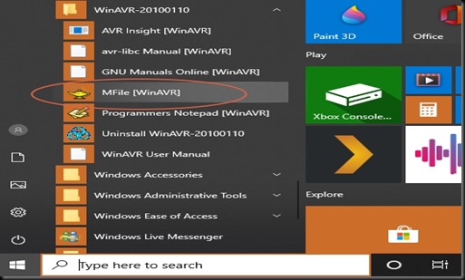
Click on MFile.


Image 12

Select  MCU Type as ATTINY85.

Image 13

Select PORT as usb

Image 14

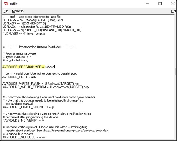
Programmer to be set as usbasp.

But usbasp is not in Programmer list.

Select any one from the Programmer list and then click on ENABLE EDITING.

Image 15

Change the Programmer as usbasp.

Image 16

Scroll up to find TARGET.

Rename TARGET to the file name of your project.Here it is ledblink.

Do not use the .c extension here.

Image 17

Save the file in the same folder where you stored the .c file.

Image 18


Under Tools  —>  click Make All

Image 11


Image 22


If no error in coding , you get Process Exit Code : 0  and .hex file created in your project folder.

Image 19

Click on Tools  –>  Program


Image 20

The .hex file will be loaded on to the ATTINY successfully.

Image 21

The LED starts blinking now.

WINAVR can be used to write C file and program using USBASP.

video :


blog_image